21st October 2022
ZVS driver
Introduction
For quite some time now I had two spare STE40NK90ZD MOSFETs and I didn't know what to use them for. After a bit of thinking I realized I could make some nice induction heater using a ZVS oscillator. After all it's quite cool to have the possibility to heat metals to such an extend where they glow red. And luckily I even had 3 very robust 1uF 1200V capacitors MPAPB1K2W10J0M6 rated for 25Arms. Furthermore I even had a coil wounded with 8mm copper tubing. Literally most of the components needed for high power ZVS driver, I ended up buying absolutely 0 components and only using those I had laying around. I also want to make the driver somewhat more sophisticated as most ZVS drivers need very high current power supply to even start-up. I want mine to be able to charge the bus capacitors first and then start oscillating. It would also be very nice if I had a button that would stop and start the driver, instead of having to cut the power every time.
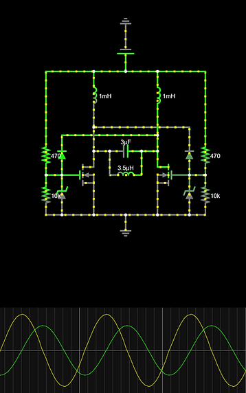
Theory behind a ZVS driver topology
The working principle behind a ZVS driver is quite straightforward, let's look at the schematics:

img.1. - basic ZVS oscillator schematics
Believe it or not but this circuit is all that it takes to run multiple hundred watts of power through the work-coil. In principle only 14 components are needed! If carefully designed we wouldn't even need R3,R4,D4,D4 for total of 10 components. So how does this work...
The key to oscillations here are asymmetries or R1 and R2. Both resistors in reality have a slightly different value. This means that Gate of one of the MOSFETs (let's say Q1) will be charged up first which makes Q1 conductive. When Q1 is conductive it's Drain to Source voltage falls down very quickly and diode D1 starts conducting as the voltage on its Anode is now higher than on its Cathode. D1 diode pulls the Gate of Q2 down, making it switched off. The resonant capacitor C1 discharges through Q1. When the capacitor is discharged, the voltage on the drain of Q2 falls under the voltage needed for D2 to conduct. D2 now pulls the Gate of Q1 down which makes Q1 switched off. Now the Gate of Q2 charges and starts conducting. This goes on and on, Q1 and Q2 pulling each other's Gates down though diodes D1 and D2. As a result the power supply keeps charging C1 and L1 and those are discharging through Q1 and Q2. As a result a tank current starts flowing in the circuit. The inductors L1 an L2 limit the power and also blocks the AC voltage from the tank circuit so it doesn't get into the power supply.
The circuit of course oscillates at the resonant frequency of the LC tank; f0 = 1/(2*pi*sqrt(L1*C1)).
I highly recommend watching the following video from Youtuber Electroboom on the subject: https://www.youtube.com/watch?v=hFJeIt_JcEc
You can also design this circuit in simulation environments such as LTspice or online simulator Falstad.
img.2. - Falstad.com simulation of ZVS oscillator
So if it works well and only needs a handful of components, why don't we use this kind of inverter everywhere? Well...
There are many disadvantages to this circuit. While it's very efficient thanks to only switching when the voltage on Drains of the MOSFETs is close to zero, it also comes with couple of inefficiencies elsewhere. For example R1 and R2 waste a lot of power. Those resistors have to charge up the Gates of the transistors at very high frequencies while they also have to provide current for D1 and D2 diodes. Also if the circuit is running above the threshold voltage of D3 and D4, the resistors also kind of act as a resistive droppers. Also due to resonant voltage rise, Q1 and Q2 have way higher voltages on their Drains than the input voltage (pi times as a matter of fact). This means that even at 30V input voltage, the peak voltage on the Drains would be almost 100V. At rectified mains voltage (325V), the voltage would climb to over 1000V! And even using for example 1200V transistors, it would not be possible to run the circuit, since it has insane inrush current and voltage transients on the power up. Sooner or later such a circuit would definitely fail. So let's sum it up...
Advantages:
- Simplicity
- Efficiency
- Low cost
- High power
Disadvantages:
- No frequency control
- Impossible to run at high input voltage
- Very high inrush
- High no-load input power
This circuit is sort of like an inverter "for dummies". It will most likely work with common transistors and it also uses low input voltages so it's hard to get hurt. But it's nowhere near an industrial grade circuit. You have no control over the oscillations, you cannot easily turn the circuit off without having to cut the power off and I wouldn't call it reliable either. In modern world we don't really like analog circuits anyway, in most cases it's better to have digital control over the circuit.
But then again... it's simplicity makes it irresistible not to build it. So I started with placing transistors on the heatsink, soldering tank capacitors to the work-coil and building the circuitry around it. The schematics for my original design stay almost the same as on image#1 but with a few improvements.
First build

img.3. - My first attempt schematics
First of all; my transistors have very high Gate capacitance of 25nF each. 10x higher than Gate capacitance of very commonly used IRFP250N. If we calculate the RC constant of commonly used 470Ohms with 25nF of capacitance we would get 11.75us. Considering the resonant frequency of my circuit is close to 50.6kHz, its one cycle only takes 19us. It would take over half a cycle for the Gates to reach acceptable voltage. That would be very inefficient as the transistors would spend a lot of their time in linear region. With my 100Ohms resistors the RC constant is only 2.5us (still a lot, but somewhat acceptable). And of course by solving one issue we get 10 more. Now the resistors heat up dramatically! They now pass a whole lot of current more than if they were higher resistance. At the input voltage of 33V the solder on the resistors started melting. Literally:
vid.1. - Melting solder with resistors
This is why I added a linear regulator to generate 24V for the resistors. At this voltage they still do get very hot, but at least they aren't smoking. Now you might ask yourselves, why did I do this? The regulator is linear it still dissipates power. Well yes, but LM317 comes in a TO220 package which can be easily mounted to a heatsink to dissipate the power, resistors have no such feature.
I also had a problem while wounding the inductors L1 and L2. During the winding one of the ferrite cores fell down from my table and cracked as ferrite is quite fragile. This crack makes its permeability lower and therefore its inductance is not as high as the inductance of my other inductor. I decided to ignore this problem as it should not create much of an issue. And thankfully, it worked just fine.
The fail of "improvement" #2
Notice how the circuit does not have any capacitors on the input and it's only using the capacitors in my power supply. This is because ZVS driver needs very high current to start up, if there were input capacitors, they would eat up all the power supply current and the circuit would not oscillate as the input voltage would rise slowly. What we need is to add input capacitance and start the circuit only after its charged. This was my first attempt to design such a feature:

img.4. - schematics with start-up circuitry
This circuit works such a way that it pulls down the Gates of the power transistors through Q2 and Q3. After some time (roughly 0.5s) Q1 starts conducting as C2 gets slowly charged through RV1. As Q1 starts conducting the Gates of Q2 and Q3 gets pulled down and therefore the Gates of the power stage are "freed". Zener diodes D5 and D6 are there just to protect the Gates from overvoltage. D5 also limits the voltage on C2 capacitor, therefore I could choose smaller cap.
While this circuit does work, it has one major flaw. The Gates of the ZVS driver need to be powered first before the input voltage is applied to the FET's Drains. Of course I didn't know about this problem beforehand otherwise I would never build it this way. I found this thanks to David Knierim during our discussion on highvoltageforum.com.
Now we can see how even such "easy" circuit can get quite complicated the more you're trying to poke into it. I had to redesign the start-up circuit.
The success of improvement #2
So since the Gates need to be powered first, I simply let them be and focused myself to the input voltage to the Drains of the power transistors. We would need such a circuit that would cut off the power from L1 and L2 inductors until input capacitors get charged and then switch the power as quickly as it is possible.
So my first thought was a relay. Adding a relay sounds easy enough, we could power the relay's inductor from the LM317 regulator. This would be very suitable for common 24V relays. Since the relay would only switch at around 24V, we would know that the input capacitors are charged to at least 26V (24V+2V LM317 dropout voltage) which is enough to start-up the circuit. This way we would not even need a timer circuit, the relay would act as a well timed circuit on its own. But then there is a huge drawback. First of all, relays are quite slow. During mechanical switching an arc is formed before the switch even switches. This arc can last for several microseconds and it does not have a low resistance. For some time before the relay switches it would deliver insufficient current and the circuit would not oscillate.
Another problem with a relay would be the huge inrush current of the circuit. While the input current of the circuit at no load is roughly 1.7A in my case the inrush current may be 100x higher. The relay must be rated for the inrush current as otherwise it would break very quickly.
Such a relay would be very expensive. Alright then, no relay...
We can do the same thing with transistors!
Using P channel FETs we can obtain "high-side" switching and connect and disconnect the input voltage however we like. Luckily I have a lot of IRFP9110 P channel FETs which are perfect for my driver. Unfortunately they feature quite high on-state resistance of 0.2ohms, which at 20A of input current would create 80W power loss. This is one of the downsides of P channel transistors, they will always have higher resistance than their N channel counterparts. Thankfully I had like 10 of these laying around so I took 4 and placed them on a heatsink where they'll dissipate 20W at 20A of input current. Not great not terrible. P channel IGBT would probably do better job here but whatever...
This is now the schematics:

img.5. - schematics with working start-up circuitry
Again the same timing principle as before; C2 gets charged through R8 which eventually charges above the threshold voltage of Q2. Q2 then switches on and pulls the Gate of Q1 down which in case of P channel transistors makes it turned on. Diodes D5 and D6 ensure that Gates of Q1 and Q2 won't get overcharged. Resistor R7 limits the current of D5. D7 diode is quite important here, its purpose is to discharge C2 every time the circuit loses power for example when power supply gets turned down. This way the capacitor needs to charge up all the way from 0V again during the next power up. A resistor between C2 and D7 might improve the lifetime of D7 as we're literally shorting out 2200uF capacitor through it every time the circuit is turned off! This way the circuit starts up reliably.
The improvement #3
Bigger bus capacitance! Think about it.. If we power the circuit from stepped down mains voltage with half bridge rectifier, we would charge the capacitor at a frequency of 100Hz. Since the circuit could draw over 20A of current, how big of a capacitance do we need so that it is acceptable?
Ripple voltage = I/(f*C). Therefore in my case: U_ripple = 20A/(100Hz*4700uF) = 42V.
42V is just too much, the voltage would drop underneath the voltage needed to run the circuit. We would need to power the circuit from at least 70V so that we could afford 42V ripple. I'm aiming to power the circuit from a little lower voltage of 50-60V. I have replaced the capacitor with a smaller 100uF capacitor and one huge 10000uF cap which will be placed next to the circuit. The 100uF cap is placed directly next to the transistors. The ripple now should be less than 20V which is not really good but it's not horrifying. This is another problem with the circuit, it uses too low input voltage and therefore we need very high currents to maintain decent output power. Higher currents will always lead to need of larger capacitors.
The improvement #4
I added yet another transistor.

img.6. - (final?) schematics
1st April 2023
Notice how we started with 2 transistors and ended up using 8?
The idea behind Q3 is that if we pull down its Gate with a button, it will pull down the gate of Q2 which will then pull up the Gate of Q1 which then finally disconnects the circuit. This way we can turn the circuit on and off with a press of a button.
I also added some LEDs to indicate the state of the circuit.
Conclusion
It's been quite some time since I started this project and just now I've realized I haven't posted any updates. I've done some minor improvements to the circuit. I added a water cooling for the primary coil as without it the coil was reaching over 200C. I have also realized I haven't posted any video of the heater in action. Unfortunately by now I have already disassembled the circuit and the only video of it was at very low power only heating up a small nail.
vid.2. - Low power (<400W) run
While this project seemed as a good idea from the start, it became less and less worth it during the development. The main benefit of a ZVS driver is that it's easy, low parts count solution. While that's true, you have very little control over the circuit and adding a simple on/off switch is a job for multiple parallel P channel transistors. It's fairly low input impedance means you need to input low voltage and it's quite hard to find low voltage very high current power supply.
That being said, I would still conclude this as a successful project. Unfortunately one final problem occurred which was the last straw.
At very high loads the N-channel power transistors are switching high currents. This means their saturation voltage Uds is rising. At some point, the on-state voltage Uds of one transistor is going to be higher than the threshold voltage of the opposing transistor. This leads to short circuit and no oscillations being produced. This happened to me at around 40A of switch current (thankfully all transistors survived).
There are some easy ways to guarantee that the Uds is going to be low enough for the circuit to work. For example we could use IGBT transistors which have (almost) constant voltage drop Uce, or this handy solution by Jakub Tejiscak. But I would only be adding another elements to already complicated circuit, at this point it's just beneficial to build some other topology for a high power induction heater.
Despite the project being a bit of a failure in the end, I definitely recommend any electronics beginner to build a ZVS circuit. It's a dirt cheap and easy driver that can provide 700W of power and more if properly built. It also shows the amazing efficiency of soft-switching and the true power of resonant circuits.