1st June 2022
Tiny (DR) Tesla Coil
Introduction
The more I work with electronics the more I enjoy to make my electronics smaller and smaller. This leads to lower parasitic properties of circuits and SMD components looks much more professional. Also using small packages and not having much space for heatsinking makes me design everything to be as efficient as possible. Therefore I have decided to try building a handheld (DR)SSTC.
Driver
As before with my SSTCs I will be using CD4046 IC to drive the coil. CD4046 generates its own programmable (with RC timer) frequency square wave. This is very handy as there is no need for feedback for the coil to work. This makes debugging easier and it's also safer as feedback can pickup unwanted frequencies from the noise being generated by the coil and surrounding electronics. This usually leads to fail of transistors. In case that 4046 loses correct feedback, it simply returns to oscillate at the set frequency.
I have designed this driver in KiCad:

img.1. - Driver schematics

img.2. - Driver PCB layout
I have designed a separate PCB with Gate-drivers, GDT and inverter. The reason for this is saving space, this driver PCB will be simply placed on top of the other board.
Inverter
The inverter board was designed to contain Gate-drivers and Gate Drive Transformer.


img.3. - Inverter schematics
img.4. - Inverter PCB layout
For Gate driver I have choose IXD(N/I)614 ICs as they already proven to me that they are very powerful and robust. I don't have much experience with low voltage MOSFETs but I think I have made a quite good job of picking up suitable FETs. I have decided to use PSMN015-60BS FETs. They should be able to handle over 200A of pulsed current but most importantly they have very low Gate capacitance, roughly 1.2nF. This is very important since the coil will be very small, it will run on high frequency. Switching multiple nF Gates at over MHz frequencies is very difficult. The Gate driving ICs would need a heatsink to charge and discharge big capacitances as these frequencies. Since I want the design to be as small as possible, heatsinks are not an option.
I left no space on my PCB for an electrolytic capacitor bank near the inverter so I had to improvise a bit. I was pleasantly surprised when I found out that even SMD ceramic capacitors in 1210 package are made with a capacitance of multiple tens of uF. I have stacked as many of 1210 package capacitors next to each other and bought 16V 47uF capacitors. This design gives me over 370uF of capacitance in ceramic SMD capacitors which are even better than electrolytic. It's worth to note that the PCB is only 7x3 cm in size!
Assembly and first tests
I would say that the finished PCB looks quite nice and professional.


img.5. - Inverter PCB top side
img.6. - Inverter PCB bottom side
img.7. - Inverter with GDT
img.8. - Inverter PCB bottom side
Unfortunately firsts tests have shown some problems. Even with only 1.2nF of Gate capacitance, at the set frequency (1.7MHz) the Gate-driver ICs are becoming quite hot after few minutes of continuous operation. Thankfully this won't be a problem as this inverter is not intended for continuous operation but rather pulsed power operation. Some of my tests were lasting longer than few minutes, during this time the IXD_614 ICs got very hot (above 100C) but that's still nothing they would not survive.
Another problem is the output voltage ringing.
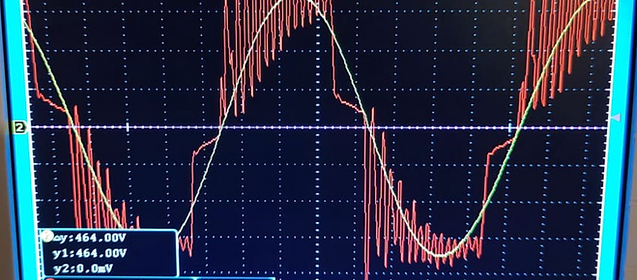
img.9. - Output waveforms (yellow - primary voltage, red - output voltage)
I hooked up the inverter to an series LC circuit with very similar resonant frequency as the output frequency of the inverter. The yellow trace is a beautiful looking sinewave measured across the resonant capacitor. Since we know the frequency, capacitance and voltage we can now also calculate the current flowing inside the circuit.
To calculate current we need to know the reactance of the capacitor which can be easily calculated: 1/(2*pi*1.7MHz*8.2nF) = 11.417ohms.
We will neglect the DC resistance of the capacitor as that's going to be substantially lower than the AC reactance. Measured 464Vpk across 11.417ohms gives a peak current of 40.64A. That is almost 19kVApk power! Of course, because of the phase shift between voltage and current, the vast majority of this power is reactive. The actual input real power measured during this test was slightly over 150 Watts.
During these tests the FETs have definitely warmed up but not as much as the Gate-driving ICs.
Still the biggest problem here is obviously the output voltage of the inverter as it has considerable ringing. This lead me to think that GDT might be saturating and causing FETs to turn off during switching. That scenario would most likely ended up in oscillations like those that can be seen on the oscilloscope.
I have put 2.2ohm SMD resistor shunt in series with the primary of the GDT to measure the primary current.

img.10. - GDT primary current ~2.3A/div
Besides some slight oscillation after the Gates (dis)charge, it's pretty much what a GDT should output during nominal operation. If the GDT was saturating, the current would rise indefinitely until the change of voltage polarity. Clearly nothing such happens here. Therefore my conclusion is that GDT is not saturating.
My another guess is that the voltage ringing is caused by poor Gate waveforms.

img.11. - GDT output voltage measured across a FET's Gate
As you can see, the leakage inductance of the GDT is too big for 1.7MHz frequency. It makes the Gate voltage oscillate a bit. Now this should not be an issue as these FETs I'm using should still be very much saturated even during the voltage drop. Since I didn't want to redesign the GDT (as I think I would not have been able to improve it much) I have decided to use damping resistors to fix the Gate waveforms. But even after the fix, the output voltage would still be the same.
I have realized a think though. The voltage oscillations on the output of the inverter have a very high frequency (>55MHz). For this high frequency I can allow for very small capacitor in RC snubber as I don't need the cut-off frequency of the RC filter to be low. Therefore I have placed an 5R6 resistor and 1nF capacitor RC snubber with a cut-off frequency of 28.4MHz. This should easily filter the 55MHz ringing while having no effect on the 1.7MHz "square wave". And these are the results:

img.12. - Output voltage of the inverter after using an RC snubber
This RC snubber works like a charm and because of the quite small capacitance and low switching voltage, the resistor doesn't even waste much power. After all these modifications the inverter board now looks like this:

img.13. - Inverter PCB bottom side

img.14. - Inverter PCB top side

img.15. - Inverter PCB side look
For now I'm quite happy with the design. It will surely be redesigned in my next revision but it does work and I can use it to drive a Tesla coil.